
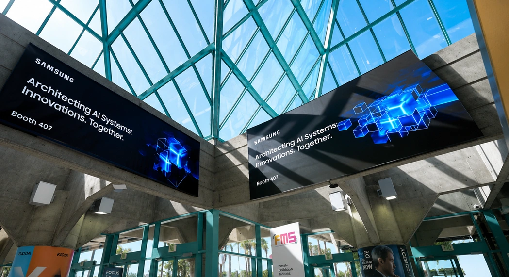
Samsung Electronics Co., Ltd. showcased a wide range of next-generation AI memory technologies at the Future of Memory and Storage (FMS) 2026, led by Samsung 3D Memory innovations. The company displayed new concept models, advanced memory architectures and enterprise storage solutions. Samsung also emphasized its long-term roadmap for AI infrastructure and high-performance computing (HPC), further showcasing its leadership in advanced memory technology.
Samsung showcased the industry’s first concept models of zHBM and zNAND-O at an event in Santa Clara, Calif. The company also debuted its V10 BV-NAND architecture with more than 400 layers for the first time. These developments are a reflection of Samsung’s continued commitment to memory technologies driven by AI. Additionally, visitors got to see nearly 30 memory and storage technologies on display at Samsung’s AI cloud server-inspired showcase exhibition booth.
During the keynote session, Jin-Yub Lee, Executive Vice President and Head of Flash Product & Technology, and Kyungryun Kim, Vice President and Project Leader of DRAM Design Team, discussed Samsung’s latest technology vision.
The keynote, “Driving the Wave of AI Revolution: 3D Innovations in Memory & Storage Architecture,” showcased Samsung’s vision to optimize AI system performance and power efficiency to meet the rapidly increasing demands of high-performance computing (HPC) and AI infrastructure.
Samsung broadens 3D memory architecture for AI computing
At the FMS 2026 conference, Samsung announced zHBM, a new memory architecture with High Bandwidth Memory stacked vertically directly on top of AI accelerators. This layout puts the processors physically much closer to the memory than the traditional layout. The architecture delivers higher bandwidth, lower latency and improved power efficiency for demanding AI workloads.
Samsung also said that future interface systems based on zHBM could achieve performance that is about eight times higher than HBM5. The company also claimed that its next generation wafer bonding technology provides more than 10x the memory density of HBM5. This leads to 3 times increase in energy efficiency and more than half decrease in thermal resistance. These improvements improve performance and operational stability for high-capacity artificial intelligence (AI) systems.
Samsung said zHBM has also been designed to support customer-specific configurations. This allows customers to implement customized intellectual property between the AI accelerator and memory layer. This flexibility allows for larger memory capacity and also improves the performance of the accelerator. Samsung also plans to work closer with customers to optimize the integration of AI processors and memory.
The company also introduced zNAND-O, a next-generation NAND solution that leverages V-NAND technology. zNAND-O is available in 4-layer and 8-layer configurations, offering a mix of high density, better I/O performance and low latency. This means the solution supports edge AI applications that need real-time processing and data-intensive work.
Industry-First V10 BV-NAND Accelerates AI Infrastructure
Samsung also showed off V10 BV-NAND based on its new Bonding V-NAND architecture. The announcement is another milestone, coming 13 years after Samsung introduced the industry’s first V-NAND technology in 2013.
V10 BV-NAND uses 400+ layers to increase storage density, while improving overall performance and power efficiency. Samsung was also able to do advanced wafer bonding to stack memory cells more efficiently. This translates into an improvement in the memory density of around 58 percent compared to the last V9 generation.
More density, but also read, write and input/output performance are increased by V10 BV-NAND. It thus meets the increasing needs of future artificial intelligence systems for high-capacity and high-speed NAND storage.
Samsung also revealed its latest AI memory roadmap including HBM4E, HBM5, LPDDR5X-PIM and PM1763. The company was the first in the industry to mass produce HBM4 in February, and began shipping HBM4E samples to customers worldwide in May. At the same time, Samsung announced LPDDR5X-PIM, the world’s first LPDDR memory with processing-in-memory technology that improves data processing efficiency and reduces power consumption.
Furthermore, Samsung also announced enterprise storage solutions such as PM1763 and BM1773 to address the rising storage requirements of AI data centers.
Samsung finally reinforced its status as the world’s only integrated device maker with memory, foundry and advanced packaging capabilities. The company’s one-stop turnkey approach offers integrated design and manufacturing services that shorten development cycles while optimizing performance and power efficiency. This will enable customers to accelerate their deployment of differentiated AI semiconductor solutions in the evolving AI era.
Explore IT Tech News for the latest advancements in Information Technology & insightful updates from industry experts!
News Source: Businesswire.com