
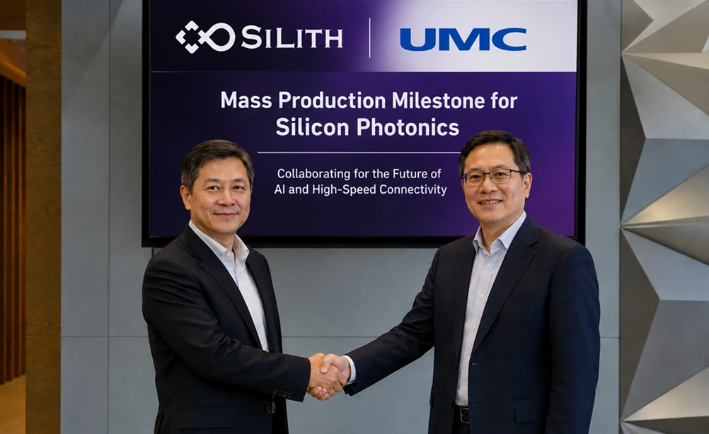
SILITH and UMC Silicon Photonics have achieved a major manufacturing milestone with the first mass-produced wafer delivered from UMC’s 12-inch semiconductor fabrication facility in Singapore. SILITH and UMC Silicon Photonics marks the transition from product development to high volume manufacturing. SILITH and UMC Silicon Photonics also deepens the partnership between the companies to address the growing demand for AI optical interconnects and hyperscale data center networks.
The partnership brings together SILITH’s silicon photonics design expertise and UMC’s large scale manufacturing capabilities. This enables customers to benefit from a scalable foundry platform with predictable production costs. It also delivers reliable manufacturing yields. The platform supports faster manufacturing timelines. Additionally, it is compatible with SILITH’s 1.6T silicon photonics technology, helping address the growing bandwidth demands of next-generation AI infrastructure.
Working together speeds up the making of AI optical interconnects
SILITH has combined its proprietary silicon photonics architecture with UMC’s silicon-on-insulator manufacturing technology and process integration expertise. Therefore, the combined engineering team delivered the platform from inception to production-ready in 18 months.
The companies state that the platform exhibited production-level performance with high yield and proven reliability. Additionally, a leading cloud infrastructure customer has qualified the technology for large scale deployment. The collaboration thus creates a manufacturing base for future demands of AI networking.
Jason Zhang, Chief Technology Officer of SILITH, said: “AI is driving an unprecedented demand for optical bandwidth, making silicon photonics a foundational technology for future data center infrastructure. At SILITH, we are building a scalable silicon photonics platform that spans pluggable optics, co-packaged optics (CPO), and future optical I/O architectures. Together with UMC, we are bringing together leading-edge silicon photonics innovation and high-volume 12-inch manufacturing to deliver the performance, scalability, and cost efficiency required for the next generation of AI networks.”
Companies Expand Future Silicon Photonics Roadmap
UMC highlighted the achievement as an important step in expanding advanced semiconductor manufacturing capabilities. Moreover, the company confirmed that its own 12-inch silicon photonics platform will become available for customer product development in 2027.
GC Hung, Senior Vice President of UMC, said: “We’re proud to partner with SILITH, a leading silicon photonics company with a proven track record of serving leading cloud infrastructure and optical networking customers, to achieve this important milestone. It reflects UMC’s ability to support customers at scale with the deep integration expertise required for complex interdisciplinary technologies such as silicon photonics. Beyond its strong 12-inch wafer manufacturing capabilities, Singapore also serves as a key technology development hub for UMC, enabling the rapid production ramp with SILITH. Looking ahead, UMC will continue to strengthen its manufacturing capabilities to support customers’ growing demand and accelerate next-generation photonics applications.”
Building on the commercialization of SILITH’s 200G-per-lane silicon photonics products, both companies are expanding their technology roadmap. They are advancing toward 400G-per-lane optical interconnects. Accordingly, they are developing a pure-silicon photonics platform using high-speed silicon Mach-Zehnder Modulators. This approach supports higher transmission speeds while maintaining CMOS compatibility, manufacturing scalability, and cost efficiency.
Beyond silicon-based modulation, UMC is collaborating with ecosystem partners to develop thin-film lithium niobate solutions for future ultra-high-bandwidth optical interconnects. Combined with advanced packaging technologies, these complementary platforms will support co-packaged optics, optical I/O, and other highly integrated architectures. They are designed to enable next-generation AI infrastructure.
Explore IT Tech News for the latest advancements in Information Technology & insightful updates from industry experts!
News Source: Businesswire.com