
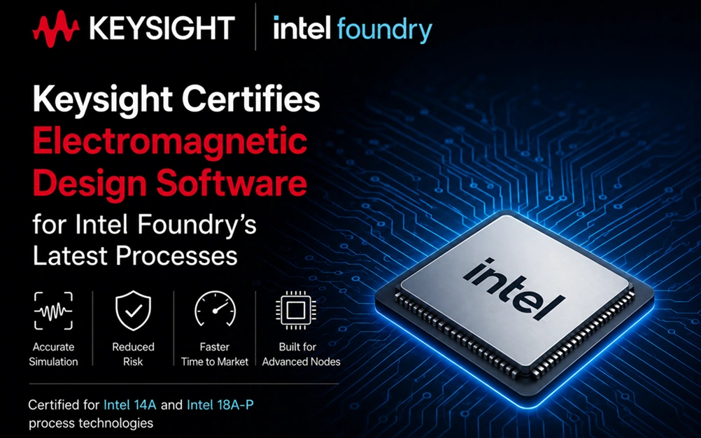
Keysight RFPro is now certified on the newest manufacturing technologies from Intel Foundry. Keysight RFPro, enabled by the The Keysight EDA Advanced Design System (ADS) now supports Intel 14A and Intel 18A-P process technologies. This RFPro certification gives RFIC and mixed-signal designers greater confidence that electromagnetic (EM) simulations accurately align with Intel Foundry’s latest manufacturing processes. Which are with Intel Foundry’s advanced manufacturing processes before production begins.
As semiconductor technology advances, engineering teams are under pressure to reduce development cycles without compromising design accuracy. Therefore, certified simulation software is more and more important in the whole semiconductor industry. It helps engineers catch performance problems early, reducing the chances of expensive design mistakes before fabrication starts.
The validated simulation tools also help organizations reduce development risks and costly redesign cycles. This enables companies to accelerate chip development and improve time-to-market for advanced semiconductor products.
Certified Simulation Powers Semiconductor Design of Tomorrow
Often, the mismatch between electromagnetic behavior and circuit performance found after tape-out results in expensive chip re-spins. Therefore, engineers need validated simulation tools before doing any design work on advanced process nodes. Keysight’s latest certification ensures confidence in simulation accuracy for Intel Foundry’s latest manufacturing technologies.
The certification comes as Intel Foundry moves forward with its technology roadmap from Intel 18A to Intel 18A-P and Intel 14A. The process technologies include RibbonFET 2 and PowerDirect, Intel’s newest transistor and power delivery architectures. This lets design teams reliably assess chip performance in the earliest stages of development.
Also, this milestone expands the long-standing collaboration between Keysight and Intel Foundry. Earlier collaborations included support for Intel 18A and EMIB-T advanced packaging technology. Together, these capabilities create a consistent design workflow across multiple Intel process generations.
Engineers developing artificial intelligence systems, high-performance computing platforms, and mobile devices can also benefit from these validated design flows. Consequently, organizations gain greater flexibility when designing next-generation semiconductor solutions.
Shawn Han, Senior Vice President and General Manager, Foundry Services, Intel Corporation, said: “As our customers look to address next-generation demands through differentiated solutions, Intel Foundry believes predictable execution on our advanced process and packaging technologies will accelerate their innovation. By collaborating closely with ecosystem partners such as Keysight to certify world-class solutions, we are providing our customers with greater confidence they can achieve their power, performance and efficiency goals and get to market more quickly.”
Niels Faché, Senior Vice President, Keysight Design Engineering Software, said: “Design teams can’t wait for a new process node to mature before they trust their simulation results. This certification means engineers can adopt Intel Foundry’s newest technologies early and get the silicon right the first time.”
The latest certification reinforces Keysight’s commitment to delivering reliable electronic design automation solutions for advanced semiconductor manufacturing. Additionally, it strengthens Intel Foundry’s ecosystem by providing designers with trusted simulation capabilities that support faster innovation while reducing development risks across future chip designs.
Explore IT Tech News for the latest advancements in Information Technology & insightful updates from industry experts!
News Source: Businesswire.com